Laser Direct Structuring (LDS) Technology
Laser Direct Structuring (LDS) is a manufacturing process in which a conductive trace can be implemented directly on an injection-molded plastic.
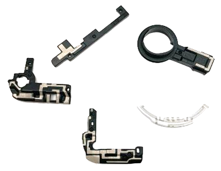
The key benefit of this technology compared to the traditional technologies (Stamped Metal or Flexible Printed Circuit) is that the LDS process allows full 3D structures, therefore enabling the flexibility to integrate complex mechanical designs in miniature 3D shapes.
This manufacturing technology is ideal when more curves are needed or less 3D volume is available. For antennas, this means the possibility to design more complex designs, reduce assembly costs or have the antenna outside the device, therefore enhancing the wireless performance while maintaining small form factors.
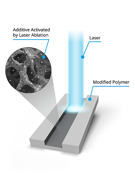
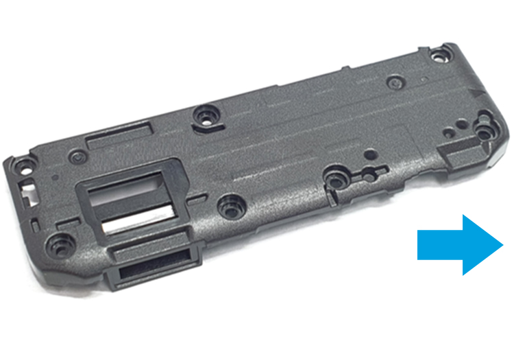
- LDS suitable resin is loaded with additives and molded to the desired shapes with traditional molding tools.
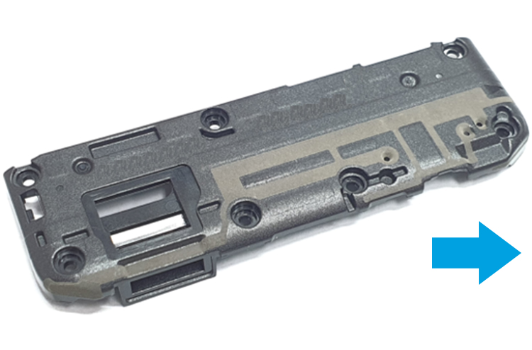
- Laser Processing machine is preloaded with the 3D pattern of the needed shape.
- The laser process activates the additives in the molded part leaving a visible “burnt” trace.
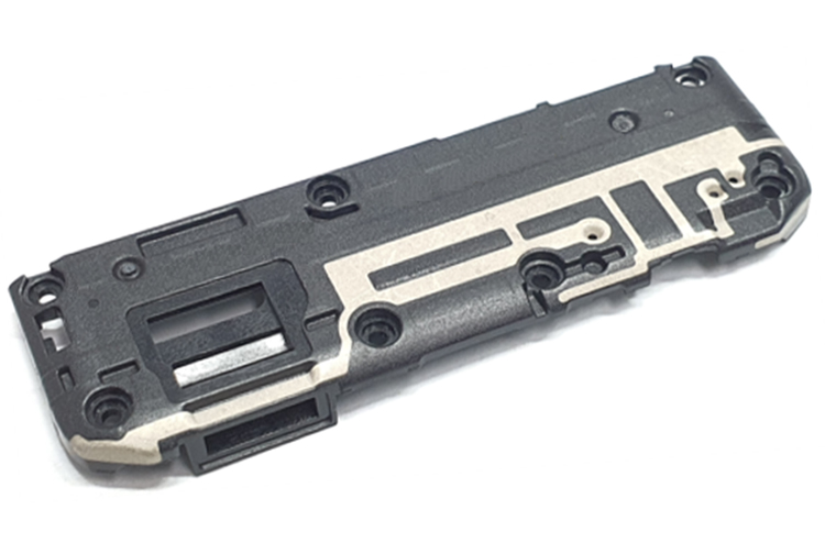
- Plating process deposits Copper (Cu) &/or Nickel (Ni) &/or Silver (Ag) &/or Gold (Au) over the lasered area to create the RF trace
Full 3D technology
- Flexibility to design smaller and thinner devices
- Conformal designs
- Multi-layer LDS | KYOCERA AVX Unique Solution!
- Possibility to design antennas directly on the device housing
- Gain 3D volume for the antennas
- save space on the board
Improved RF Performance
- Combine several antennas on the same 3D structure
- Increase the distance between the antenna and other components
- Unique antenna patterns and shapes
Manufacturing Advantages
- Flexibility to optimize the pattern design without additional tooling costs
- Reduction of assembly costs in mass production
- Light weight
- SMT (Surface Mount Technology) possible for antennas
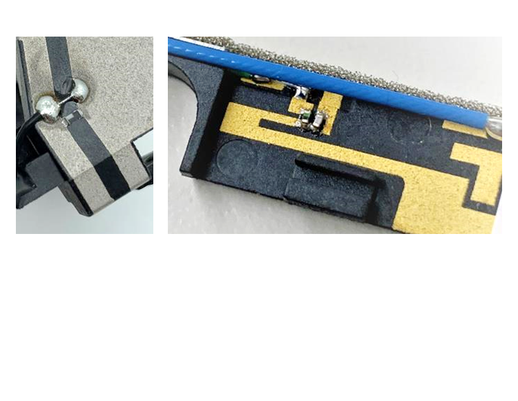
- Soldering of SMD components (e.g. matching components) or cables possible
- Painting process for cosmetics available

| Design Process with RF simulation tools (HFSS, CST) | |
| 3D CAD modelling design/review/mechanical fitting | |
| Soft-tooling for carrier | 2 Weeks |
| Hard-Tooling for carrier | 5 Weeks |
| Jig / Fixture for Laser processing | 1 Week |
| Laser processing + Plating | 2-3 Days |
| Painting & Masking | 2-3 Days |
| Samples for testing RF (Soft Tool) | 2 Weeks |
| Design iteration | 2-3 Days |
| SMT / Cable assembly / mechanical integration | Few Days |
The process of LDS consists of 3 major phases: Injection Molding, Lasering Activation and Metallization. In some cases, there are additional steps like SMT process or soldering for the assembly of components. For deeper insights into the LDS process, check out the whitepaper: Working Principles & Benefits for RF Applications
Injection Molding
Laser Activation
Metallization

Please accept YouTube cookies to play this video. By accepting you will be accessing content from YouTube, a service provided by an external third party.
If you accept this notice, your choice will be saved and the page will refresh.
can make your project a reality?

